Lenz LZV100 Repairs
The 3 most common issues with the LZV100 are the battery is flat, an older version (before 3.6) of XpressNet and no DCC output or short circuit. Other faults will need more investigation and may not be repairable. The XpressNet AB signal comes from the 68 pin CPU (which needs a buffer, RAM, ROM, and crystal to work), through an RS485 chip, over a short ribbon cable to the sockets. The RS485 chip may be easy to replace, but the CPU would need special tools.
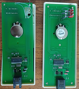
Inside the LZV100 are 2 PCBs joined by a short ribbon cable. The top board has the PQRS connector and the main CPU. The CPU has either an ultraviolet erasable EPROM or a onetime PROM with the program in it. The label gives the version and covers the UV window. Next to the PROM is the RAM chip and backup battery. The lower board is the booster and has the power input and DCC output connector UVJK. The DCC output uses an FET bridge circuit to drive up to 5 amps.
ER97 : The battery is flat.
The installed battery has a long life, but it‘s soldered in. It should be about 3 volts, if it close to 2 volts it needs replacing. It‘s a CR2450 with 600mAh capacity and a direct replacement is hard to find. Simpler and easier is to use a CR2032 with 225mAh capacity and a battery holder. Since this is a very common battery it should be easy to buy and slide in future. You may need to do a reset after replacing the battery.

Version 3.6 upgrade.
Version 3.0 only had 13 functions F0 to F12 and 255 CVs, 3.5 may also have had 13 functions and 999 CVs, 3.6 has 29 functions and 1024 CVs. This upgrade is simple if you have a copy of a 3.6 chip. Slide a slim screwdriver between the chip and the socket to lift out the old chip and push in the new chip. A small indent in one end shows which way round it should be inserted. If the old chip has a round window under the label, it can be erased and re-programmed with the current version. You need a UV eraser, universal programmer and a working 3.6 chip to copy. The UV erasable chip is an 27C256 with 32k bytes. It takes about 15 minutes under a strong UV lamp to erase the old contents. After re-programming the window needs to be covered as sunlight can start to erase the program. You may need to do a reset after upgrading to 3.6.
Lenz LZV100 reset.
The Lenz instructions are:
1) Set your handheld to operate locomotive 00 (the analog locomotive)
and bring that locomotive to a stop.
2) Press the F4 key 25 times in succession. You may notice that after the 20th time
that brief power interruption occurs on the layout.
3) Remove power from the LZV100 by turning off power to the transformer (not ST key).
Unfortunately, it seems to need 25 of "F4 on", after 20 "F4 on"s the redlight goes off
for a half a second. Since the F4 mode is usually toggle, (not momentary)
it also needs 25 "F4 off"s, making 50 presses of the F4 key.
If you watch the red LED, you can tell if 25 or 50 are needed.
FET change.
These are on the booster PCB. The only difference between the PCB in the LV102 booster unit and booster in the LZV100 seems to be the missing 20 pin ribbon connector, LMAB connectors and 12 volt regulator.
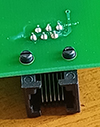
If you put the power into the wrong pins or have an associated booster and connect it the wrong way on the J and K pins it will probably blow 2 of the 4 output FETs. This usually results in a short circuit that will not clear or only half the voltage out. These FETs are the 4 x FDS6912A on the booster PCB near the edge with the connectors. They are very cheap at £6 for 10, easy to break, very small and hard to replace. They are rated at 30 volts and 6 amps, and each chip has 2 FETs inside and these are wired in parallel.


Black soot (left photo) and/or lumps in the plastic (right picture) indicate which FETs need to be replaced.
Google "SMD chip replacement" or "SMD rework" for hints on replacing these. Also there are SMD (surface mount device) practice kits on Amazon, eBay and MERG. The first step is to remove the damaged chips without damaging the PCB or the nearby resistor. The PCB can de-laminate at temperatures above 120°C so take care and be quick if using a soldering iron at 300°C or more with 180°C solder or 220°C lead free solder.
These chips are about 6mm square and getting all 8 legs unsoldered at the same time without getting the PCB tracks too hot and melting the attachment to the fibreglass base is very difficult. I find it is best to carefully cut some of the legs on the chip using small wire cutters. Take care as the PCB may already be damaged when the chips were blown. The 4 legs on the side nearest the connector are all on a large PCB land and easy to cut. There is a thin PCB track joining pins 2 and 4 (the gate pins) which is the most likely to lift. So, I carefully cut pins 1 and 4 putting as little stress on the PCB as possible. Unsolder pins 2 and 3 (also pins 6 and 7) and remove the chip. The pads then need to be cleaned up, and leg parts removed.
For a quick test after removing the faulty chips, the 2 boards can be powered up with a controller, and the short circuit should have gone. Power down again to add the chips. Apply some electrical flux, carefully position the new chip and solder in using a small bit in the iron, making sure the pin 1 mark is in the same place as the other FETs and that there is no solder bridge across any pins. Good lighting, magnification and a good soldering iron are necessary.
Hot air SMD rework tools are good, but only for SMD work, you can‘t use them for anything else. You also need solder paste which you can apply very small amounts via a small needle, and this has a shelf life of about 6 months before it goes too solid to use. It also has a lower melting point (140°C) making PCB damage less likely. Using hot air and solder paste, the components tend to centralize themselves on the pads using surface tension.
XpressNet Interface
The 5 pin Din and 4 pin LMAB sockets combine on the PCB. The L and M is a low current 12 volt supply, which is fed via small inductors to block RF interferance. They can only handle a low current and are easily blown open circuit, if the controllers are blank when plugged in this a probable cause. There are no markings on the devices which are about 2.5mm square. Try a CD32 10uH ? but it's a little hard to solder in.
The A and B lines are more complex, the first device looks like a small (100mA) polyfuse. It seems to be 10 to 20 ohms but current polyfuses are less than 5 ohms. Probably should be OK, but try Bourns MF-R005 ? The next device on the A and B lines, is a small cylinder TVS (transient voltage suppressor) diode, marked Z and 7.5, so probably limits to about 7.5 volts. These are to suppress damaging voltages on the inputs, and may fail as a short circuit. Try Vishay SMBJ7.5D-M3/H ? These are slightly too long and too close to the LMAB connector making it difficult to replace. The final device on this PCB is another of the small unmarked inductors, one on each line. Hopefully all those components should prevent any damage passing further in. The A and B connections then pass over the ribbon cable to the other PCB which has the termination and bias resistors as well as the SP485CN RS-485 transceiver chip.
LH90 Repairs
There are at least 2 versions of the software, the main difference is the number of functions. It was upgradeable by connecting it to a Windows 2000 PC and using HyperTerminal, but I've been unable to find out any more details.
To open the LH90, remove 5 screws which may be either small posidrive or Torx T9. The large speed knob just pulls off or can be eased off with a flat screwdriver.
LH90 Socket
The LH90 cable socket can be replaced if it fails either with bad connections or the cable does not click in securely. The socket is a low profile RJ12 6p6c. 2 connections are used for the XpressNet A and B, 2 for the 12 Volt power, and the other 2 are probably used when doing the upgrade to the software in the LH90.
Open the LH90, the PCB can then be removed but will remain attached to the direction switch and case by 3 thin wires. Take care not to trap or stress these wires as it is easy to break the connections.
To remove the old socket, first cut off the ends of the 2 plastic fixings that hold the socket to the PCB. Then use plenty of solder on the 6 pins to remove the old socket. Use solder wick to clean up all the solder from the 6 holes. The new socket can then be pushed in and soldered up.
LH90 Switch
If the direction switch breaks or fails and needs to be replaced, open the case as above and remove the knob. Make a note of the 3 switch connections, and then unsolder them and remove the pcb. The switch is held on by a nut which is under the grey display filter. The filter is held in by small molded lugs on the ends. As the lugs make the filter slighty longer than the window push the filter out by bending it the near the middle.
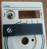
The nut can then be undone and the switch replaced, the switch is a minature toggle switch ON/OFF/ON (not the momentary type). The display filter can be replaced by bending it in the middle until it clips in. Make sure the wires remain free and replace the PCB in the case then fit the knob to hold it all together.
There are 2 versions of the PCB, V1.0 has the 3 connections below the switch, left to right are bottom, middle and top. V2 has the more obvious connections alongside the switch contacts. The 3 wires can be re-soldered and the case re-assembled.